WAT(Wafer Acceptance Test)與WS or CPY(Wafer Sort or Chip Pobing Yield)的定位與目的
WAT在製程研發與產品量產階段的不同目的
1. SBU : 市場需求, 成本考量
2. TD : 提供Design rule, 原件特性
3. RD : 元件模擬, 線路設計
4. 研發 : 元件特性是否如預期模擬
5. 量產 : 監測製程是否有缺失, 追查原因
每個die之間的切割道會放上PCM或WAT test key 作為監測生產線上製程穩定性和元件電性
WAT fail 影響有多大? 兇手是誰?
1. WAT fail 可能一點事兒也沒有
--測試 Issue
--WAT spec 不一定是 real spec
--WAT window by product 不同
2. WAT fail 可能只是單批事件
--整合部的X檔案
3. 不過WAT fail也可能是冰山一角
--前段製程Shift (ML1 WAT)
--機台不定時秀逗
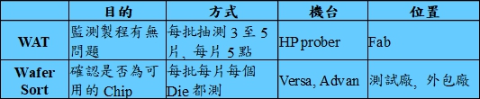
從產品觀點與製程觀點來看Wafer Sort的主要分類
製程觀點
--Defect, CD異常, IMP異常, Film異常, Over Etch, Under Etch....
產品觀點
--速度, 漏電
--Fab 常常被要求Tighten spec的無奈
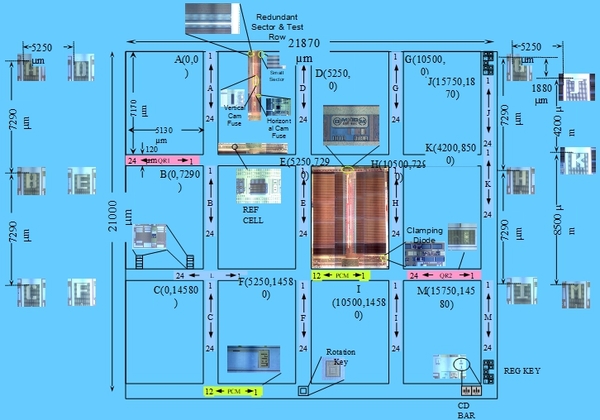
WAT Contents:
Diode -- Forward voltage, -- Inverse leakage
Transistor -- NFET, PFET, Array FET, -- VT_NODE
Capacitor -- Oxide cap. -- Overlap cap. -- Junction cap. -- Trench cap.
Resistor -- Sheet rest. -- Contact rest. -- Contact chain rest.
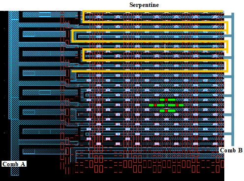
APDM* -- Leakage to all, -- Open yield, -- Short yield
*The APDM (Array Process Diagnosis Monitors) is based on a large cell array. The layout is similar to the product despite the outer connection of GC, M0, M1 and M2. The wiring scheme using combs and serpentines allows the investigation of the short and open yield of particular level.
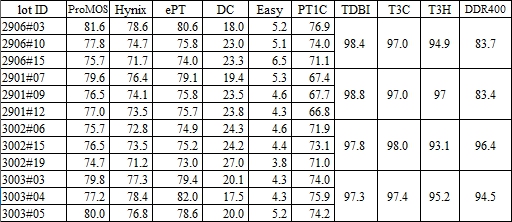
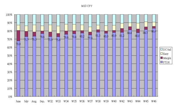
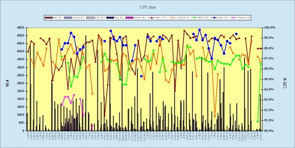
以下圖表表示試產的良率因測試程式不同而結果不同, 所以良率測試除了要揪出產線的問題, 也要考慮是否誤殺的問題!另一個重點是每週良率趨勢圖, 晶圓廠幾乎所有的活動都是圍繞良率改善的議題在打轉!